Exciton valley character in 2D semiconductors - New TRR 227 paper published in Nature Communications
TRR 227 researchers at Freie Universität Berlin discovered a way to use nanomechanics to control and study hidden intervalley excitons in two-dimensional semiconductors. This breakthrough provides a new material science technique to understand band structure, control spins and valleys, and suggests a new approach for manipulation of spin/valley-based information and its storage.
News from Sep 09, 2024
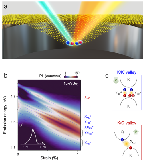
Figure caption:
(a) Cartoon of a suspended and controllably stretched 2D material. A laser light creates excitons, bound electron-hole pairs, inside the material. (b) False color photoluminescence map vs. strain in a 1L-WSe2. Different peaks in this map correspond to different excitons. Researchers found that the rate of shift of these excitonic peaks with strain provides exciton’s valley information. (c) Cartoon representation of different valleys hosting excitons. Different strain response of different excitons (e.g., KK and KQ) leads to their coupling at a specific strain value, 0.35%, leading to their optical brightening.
Scientists at Freie Universität Berlin (B08 and B07; leading authors Abhijeet Kumar, Denis Yagodkin, and TRR PIs Kirill Bolotin, Cornelius Gahl) discovered a way to use nanomechanical manipulation to “brighten” and study normally inaccessible “dark” intervalley excitons in two-dimensional (2D) semiconductors. Properties of these materials relevant for applications in spin/valley-tronics are dominated by strongly bound electron-hole pairs, known as excitons. These excitons feature long lifetimes, unique transport properties, and strong interactions – attributes that ignited immense interest in 2D materials during the last decade. However, the majority of the excitons remain hidden from the optical probes (hence, “dark”), hampering their applications.
The research team, led by Prof. Kirill I. Bolotin, discovered a technique to manipulate the band structure, control the energy hierarchy of excitons, and increase their interactions with light by mechanically stretching the 2D semiconductors. Moreover, they pioneered an approach to identify the type of dark excitons in WSe2 and WS2, two common 2D semiconductors, by studying their response to stretching.
The implications of this research extend beyond the fundamental science. The ability to engineer the valley properties of excitons in 2D materials opens new possibilities for creating next-generation spin/valley-tronic devices for computation with ultralow power consumption. The group also demonstrated large energy tuning of single photon emitters that may find extensive application in quantum communication.
In summary, this pioneering work in strain engineering of 2D semiconductors offers a powerful new tool for scientists and engineers. The technique is ready to advance the understanding of spin and valley dynamics, engineer materials with desired properties, and uncover new excitonic states in other systems.
These results were recently published in Nature Communications.
A. M. Kumar, D. Yagodkin, R. Rosati, D. J. Bock, C. Schattauer, S. Tobisch, J. Hagel, B. Höfer, J. N. Kirchhof, P. Hernández López, K. Burfeindt, S. Heeg, C. Gahl, F. Libisch, E. Malic, and K. I. Bolotin: Strain fingerprinting of exciton valley character in 2D semiconductors - Nat. Commun. 15: 7546 (2024) - DOI: 10.1038/s41467-024-51195-y

